
UPSC Mapping
| Prelims | Mains |
|---|---|
| Science & Tech | GS Paper 3 |
What is Semicon 2.0?
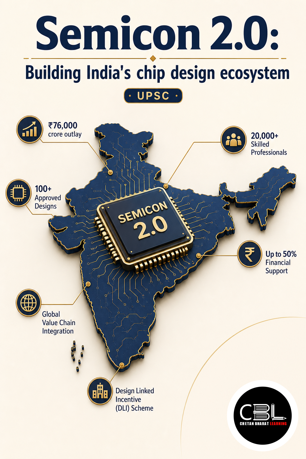
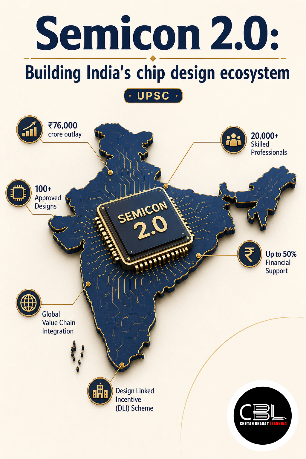
Semicon 2.0 represents the second phase of the India Semiconductor Mission (ISM), expanding support beyond physical fabrication plants (fabs) to cover the entire semiconductor value chain. The programme specifically targets chip design, intellectual property (IP) creation, electronic design automation (EDA) tools, and advanced packaging.
Why is Semicon 2.0 in News?
The Ministry of Electronics and Information Technology (MeitY) recently notified the operational framework for the Rs 1.27 lakh crore scheme. The guidelines explicitly open up commercial chip-design incentives to companies owned and controlled by Overseas Citizens of India (OCIs), leveraging their global experience to build advanced design companies in India. The scheme also introduces deployment-linked incentives to guarantee initial market adoption by subsidising electronics manufacturers to switch from established overseas suppliers to home-grown chips.
Key Features
- Deployment-Linked Incentive: Fabless companies receive 9% of net sales for five years, capped at Rs 30 crore per product and Rs 120 crore per company.
- Strategic vs Commercial Tracks: Track 1 funds chips for national security; Track 2 supports consumer/industrial markets.
- Startup Seed Funding: Up to Rs 15 crore (50% of project cost) for eligible startups and MSMEs.
- Royalty Financing: 5% of net revenue until 1.5× government assistance is recovered.
- Materials & Equipment: 30% capex support for wafers, substrates, chemicals, gases; declining PLI for equipment manufacturers.
Challenges
- Capital Intensity: High capex with long gestation periods.
- Supply Chain Monopolies: Critical EDA tools and photolithography equipment remain concentrated abroad.
- Market Trust Deficit: Convincing global OEMs to adopt new Indian chips is difficult.
- Talent Retention: Domestic hardware ecosystem is still nascent, prompting brain drain.
Way Forward
Mandate indigenous chips in government telecom and defence procurement to guarantee demand. Provide patient deep-tech capital and strengthen university-industry linkages to translate academic research into commercial patents. This unified approach will accelerate India’s transition towards a self-reliant technological powerhouse.
Prelims Practice Corner
- Q1. What is the total financial outlay approved for the Semicon 2.0 programme?
(a) Rs 76,000 crore (b) Rs 1.27 lakh crore (c) Rs 2.5 lakh crore (d) Rs 50,000 croreCorrect Answer: (b) Rs 1.27 lakh crore
- Q2. Under the deployment-linked incentive, what percentage of net sales is reimbursed?
(a) 5% (b) 9% (c) 15% (d) 25%Correct Answer: (b) 9%
- Q3. Which investors are newly eligible for commercial chip-design incentives under Semicon 2.0?
(a) FPIs (b) OCIs (c) Sovereign Wealth Funds (d) Multilateral BanksCorrect Answer: (b) OCIs
- Q4. What is the maximum seed funding available for eligible startups and MSMEs?
(a) Rs 5 crore (b) Rs 10 crore (c) Rs 15 crore (d) Rs 50 croreCorrect Answer: (c) Rs 15 crore
- Q5. What does ‘fabless’ refer to in semiconductors?
(a) Raw silicon manufacturers (b) Design-only firms outsourcing fabrication (c) Govt labs (d) EDA developersCorrect Answer: (b) Design-only firms outsourcing fabrication
Mains Practice Questions
- Discuss the significance of the ‘deployment-linked incentive’ in overcoming market entry barriers for domestic fabless semiconductor companies. (10 marks)Answer Structure:
Intro: Define fabless model and India’s design engineering strength vs. IP ownership weakness.
Body: Explain the ‘chicken-and-egg’ problem and how 9% reimbursement de-risks adoption.
Conclusion: State-backed market creation is essential for strategic deep-tech ownership. - “True technological sovereignty in semiconductors requires a complete domestic ecosystem, not just fabs.” Analyze in context of Semicon 2.0. (15 marks)Answer Structure:
Intro: Introduce Semicon 2.0’s Rs 1.27 lakh crore package and upstream focus.
Body: Discuss EDA tools, core IP, ATMP, OA inclusion, royalty financing for R&D.
Conclusion: Leverage India’s software/engineering talent for niche design leadership.
FAQs on Semicon 2.0
Why is chip design considered more critical than manufacturing?
Design and IP carry strategic value and ensure sovereignty; mere assembly leaves countries vulnerable to supply shocks and export controls.
How does the scheme support semiconductor materials manufacturing?
Up to 30% capex support for facilities producing wafers, substrates, chemicals, and gases, reducing reliance on imports.
What is the ‘royalty financing’ model?
The government provides upfront capital; companies pay 5% of net revenue until 1.5× the initial assistance is repaid, aligning returns with commercial success.
Related Current Affairs
Preparing for UPSC, PCS or HCS?
Talk to a mentor at Chetan Bharat Learning, Chandigarh. Free guidance on choosing the right exam and building a study plan.
Chat on WhatsAppCall 97793 53345UPSC / IAS / PCS coaching in Chandigarh · Trusted by aspirants across Punjab & Haryana
Leave a Reply
You must be logged in to post a comment.